
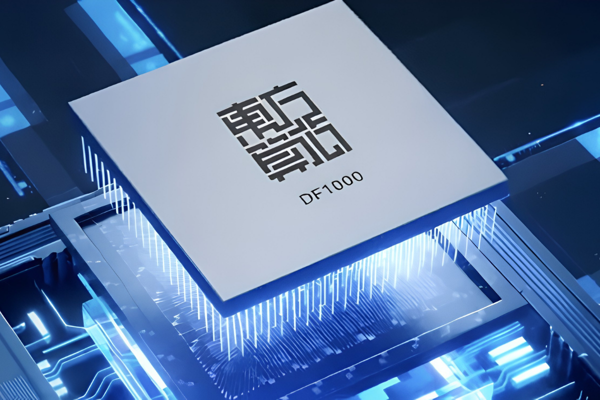
Oriental Compute Core Unveils DF1000: Advancing AI Hardware with 3D Hybrid-Bonded Packaging
Chinese AI chip startup Oriental Compute Core has officially debuted its new DF1000 chip, marking a significant milestone in semiconductor architecture. The DF1000 distinguishes itself through the use of DRAM-logic wafer-level hybrid-bonded 3D packaging technology. This sophisticated design is specifically engineered to provide higher bandwidth, addressing the critical data transfer bottlenecks currently facing high-performance AI applications. By integrating DRAM and logic components at the wafer level, Oriental Compute Core aims to optimize the efficiency of data movement within the chip. This announcement highlights the growing trend of utilizing advanced 3D packaging techniques to enhance the capabilities of next-generation artificial intelligence hardware, positioning the DF1000 as a notable development in the competitive AI chip landscape.
Key Takeaways
- Debut of DF1000: Oriental Compute Core has officially introduced its latest AI chip, the DF1000, to the market.
- Advanced 3D Packaging: The chip utilizes DRAM-logic wafer-level hybrid-bonded 3D packaging, a cutting-edge manufacturing technique.
- Focus on Bandwidth: The primary objective of this specific architectural choice is to achieve higher bandwidth for AI processing.
- Integration Strategy: By bonding DRAM directly with logic at the wafer level, the design minimizes the physical distance data must travel.
In-Depth Analysis
The Architecture of the DF1000
The debut of the DF1000 by Oriental Compute Core represents a strategic shift toward advanced packaging solutions in the AI semiconductor sector. At the heart of this development is the use of DRAM-logic wafer-level hybrid-bonded 3D packaging. Unlike traditional 2D chip designs where memory and logic units are placed side-by-side on a substrate, 3D packaging allows these components to be stacked vertically.
The "wafer-level" aspect indicates that the bonding process occurs while the components are still in their wafer form, rather than after they have been individualised into separate dies. This method allows for a much higher density of interconnects between the logic (the processing unit) and the DRAM (the memory). By utilizing hybrid bonding, the DF1000 can achieve a direct metal-to-metal connection without the need for traditional solder bumps, which significantly reduces the pitch between connections and enhances the overall structural integrity and thermal performance of the chip.
Overcoming the Memory Wall with Higher Bandwidth
The most critical advantage cited for the DF1000's architecture is the attainment of higher bandwidth. In the realm of artificial intelligence, particularly with large-scale models, the "memory wall"—the gap between how fast a processor can operate and how fast it can access data from memory—is a major performance bottleneck.
By employing DRAM-logic hybrid bonding, the DF1000 effectively shortens the communication path between the processing logic and the data storage. This vertical integration allows for a massive increase in the number of parallel data paths (interconnects), which directly translates to higher bandwidth. This means the DF1000 is designed to handle the intensive data throughput required for modern AI workloads more efficiently than chips relying on conventional packaging. The focus on bandwidth suggests that Oriental Compute Core is targeting applications where rapid data movement is as vital as raw computational power.
Industry Impact
The introduction of the DF1000 signals a broader industry move toward 3D integration as a standard for high-performance AI hardware. As traditional scaling (Moore's Law) becomes increasingly difficult and expensive, semiconductor companies are looking toward "More than Moore" strategies, such as advanced packaging, to deliver performance gains.
Oriental Compute Core’s adoption of wafer-level hybrid bonding places them at the forefront of this technical trend. This approach not only improves bandwidth but also offers potential benefits in power efficiency and form factor reduction. For the AI industry, the success of such chips could lead to more capable edge devices and more efficient data center accelerators. Furthermore, this development underscores the intensifying competition in the global AI chip market, as startups leverage specialized architectural innovations to challenge established players and meet the specific demands of the AI era.
Frequently Asked Questions
Question: What is the main technical feature of the DF1000 chip?
The DF1000 chip features DRAM-logic wafer-level hybrid-bonded 3D packaging. This technology allows for the vertical stacking and direct bonding of memory and logic components at the wafer stage, which is designed to provide significantly higher bandwidth compared to traditional packaging methods.
Question: Why is higher bandwidth important for AI chips like the DF1000?
AI workloads involve processing vast amounts of data at high speeds. Higher bandwidth ensures that the logic units of the chip are not left waiting for data to arrive from the memory, thereby reducing latency and increasing the overall efficiency and speed of AI computations.
Question: Who is the manufacturer of the DF1000?
The DF1000 is developed by Oriental Compute Core, a Chinese AI chip startup focused on utilizing advanced semiconductor packaging technologies to enhance hardware performance.

